


Our son got lots of new toys over the Christmas period. One of his favourites is a plastic guitar with buttons on the fingerboard, lots of lights, and even a whammy bar1. It’s really fun. At one year old he’s much too young for a computer, but many of his toys, including the guitar, have computers inside them. But, of course, we usually don’t call them computers. Instead, they are ‘microcontrollers’.
A moment’s thought tells us that microcontrollers are everywhere: in our homes, in washing machines, refrigerators and microwaves, in our automobiles, and many, many other places. And some of these microcontrollers are based on designs that have been around for decades. I don’t dare risk opening up the toy guitar – he would be very upset – but I wouldn’t be surprised if the microcontroller inside uses an 8-bit architecture that was first developed in the 1970s. Prompted by my son happily playing with his new toy guitar, it seems like a good moment to delve into the history of the ubiquitous, but often invisible microcontroller.
Before we delve into the history of the microcontroller, we need to define what it is. Wikipedia defines the microcontroller as a ‘small computer’ on a single integrated circuit. This distinguishes it from a microprocessor, which is just a Central Processing Unit on a chip and needs additional integrated circuits to create a functional computer, and a ‘System-on-Chip’ or ‘SoC’ which is the term used when the computer isn’t judged to be ‘small’.
It’s perhaps surprising that the earliest microcontrollers emerged at about the same time as the first microprocessors. One might expect that it’s significantly harder to build a complete computer on a single integrated circuit when compared to just a CPU. However, the earliest microprocessors were often used in designs which needed very small amounts of ROM or RAM and which were highly price-sensitive. Engineers were soon able to overcome the technical challenges of adding a small amount of memory and input/output circuitry alongside a processor. And the potential commercial benefits for the system designer from the lower costs associated with using a microcontroller were considerable. As a result, there was a large market for microcontrollers and many of the leading semiconductor manufacturers in the 1970s and 1980s had their own line of microcontrollers, sold alongside their microprocessor designs.
Microcontrollers have typically had a lower profile and attracted less attention than microprocessors, for two reasons. First, the need to keep integrated circuit die sizes small whilst also accommodating memory and input/output, has meant that their CPUs have been less sophisticated than contemporary microprocessors. Second, they have typically been used in systems where users cannot read or change their code. So whilst different generations have grown up with access to ‘home’ and then ‘personal’ computers or workstations, and have become familiar with the architectures of the microprocessors powering these machines, microcontrollers have been locked away, hidden inside calculators, toys, automobiles and domestic appliances.
As semiconductor node sizes shrank over the years, it became possible to use existing microprocessor designs as the CPU part of a microcontroller. These CPUs typically had higher performance, richer software ecosystems, and were easier to program than the earlier designs, which had been designed especially for early microcontrollers, that they replaced. Today, most microcontroller designs incorporate a processor either from the 8-bit era (e.g. Z80, 6502), or the 16-bit era (e.g. 68000) or are modern 32-bit designs (such as ARM Cortex or RISC-V).
This is the first post in a series on the earliest microcontrollers. We’ll look at some of the leading designs of the time, their history and where they were used. Although these designs have had a much lower profile than the early microprocessors, they played a key role in making computing ubiquitous.
Before we get to real microcontrollers, it’s worth discussing the “idea” of the microcontroller. In the 1960s, as more and more components were crammed onto integrated circuits, it became increasingly obvious that it would soon be possible to create a ‘computer on a chip’.
In 1970 Gilbert Hyatt filed a patent for a ‘microcomputer architecture … that facilitates a fully integrated circuit computer on a single integrated circuit chip.’ Or, in other words, a ‘microcontroller’. It took two decades for that patent to be granted. The Los Angeles Times reported2 in 1990 that:
In July, after a 20-year legal fight that generated an estimated 10,000 pages of paperwork, the U.S. Patent and Trademark Office gave Hyatt patent No. 4,942,5163 for a “Single Chip Integrated Circuit Computer Architecture.” The patent shocked the electronics world.
The LA Times reported its conversation with Hyatt::
“I didn’t invent the computer, but I came up with a very good improvement,” said Hyatt, a 52-year-old workaholic who prefers to work alone at a modest home in a cul-de-sac in La Palma. “My work in those days led to the PCs of today.”
Hyatt had technical expertise, having graduated from UC Berkeley and worked at electronics conglomerate Teledyne, and had attempted to develop his ideas, raising capital before falling out with his investors. However, according to one former colleague4:
Hyatt was a stubborn, impractical researcher without a viable technology who was obsessed with “paper rights.”
After the 1990 patent approval, Hyatt was able to claim tens of millions of dollars in royalties, from Sony and other major companies. However, other firms continued to challenge the patent approval, until, in 1996, a central claim of Hyatt’s relating to the ‘invention’ of the microcontroller was overturned5.
“After a five-year review of tens of thousands of pages of documents, the patent office ruled that Hyatt did not describe a microcontroller until 1977, in one of many amendments known as a continuation.”
Hyatt was later involved in another set of legal cases, this time relating to millions of dollars of potential tax liabilities and related damages, that made their way to the US Supreme Court and would finally be resolved only in 20196.
In a 2014 interview7 Hyatt was quoted as saying:
“I felt that the industry had taken my technology and, not only hadn’t rewarded me, but hadn’t given me recognition until my patents started to issue,” Hyatt said.
The reality, though, is that he didn’t have access to the technology required to create a working microcontroller and probably wouldn’t have been successful in creating one if he did.
Leading the challenge to Hyatt’s patent was Texas Instruments (TI). TI started life in 1951 following the reorganisation of ‘Geophysical Service Incorporated’, a Dallas company that made seismic equipment for the oil industry and which had expanded into electronics. In 1952 TI purchased a licence to make Germanium transistors from Western Electric, the manufacturing arm of AT&T, whose Bell Labs research arm had invented the device. TI quickly became a pioneer in the development and commercialisation of semiconductors and related technology. The first transistor radio in 1954 was followed by the first integrated circuit in 1958 and the, hugely popular, 7400 series of ‘Bipolar’ Transistor-Transistor-Logic or TTL integrated circuits in the early 1960s. By the start of the 1970s TI was a semiconductor giant with revenues of around a billion dollars.
In the late 1960s, TI’s attention had turned to using integrated circuits to shrink ‘desktop’ calculators. Early electronic calculators used discrete transistors and so were heavy and needed AC power supplies. They were an obvious commercial application for increasingly powerful integrated circuits. In 1967, at the end of a two-year project, a TI team led by Jack Kilby developed and, was granted a patent8 on, the first first ‘pocket’ calculator, known as the ‘Cal Tech’ (perhaps surprisingly named after the California Institute of Technology). ‘Cal Tech’ reduced the hundreds of discrete transistors in earlier calculators down to just four integrated circuits. The National Museum of American History has the first Cal Tech calculator9 inscribed with the date (March 29, 1967) when it was presented to TI’s president, Pat Haggerty.
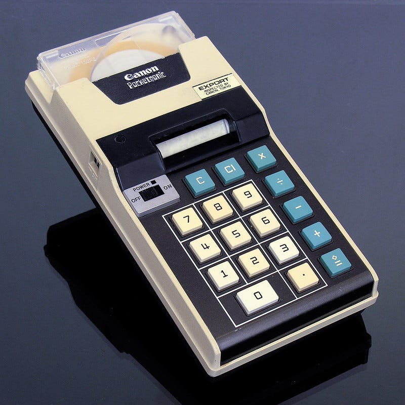
TI would go in to work with Canon to turn the Cal Tech’s technology into a commercial design, known as the ‘Pocketronic’ which appeared in 1970 (which despite its name would have been hard to put into most pockets).
From the perspective of 2024, it’s quite hard to take in how big a deal the emergence of small electronic calculators were in the early 1970s. Arithmetic is fundamental to many jobs, from basic accounting for small businesses to complex engineering. Prior to the development of the affordable, portable electronic calculator, these needed to be performed by hand (with variable accuracy) or using an expensive and unwieldy, transistor based, electronic or electro-mechanical desktop calculator.
There was a huge potential market for cheaper and more portable calculators. Their development calculators would soon become a race between major US and Japanese semiconductor and electronic companies. This, in turn, was a central part of the wider competitive struggle between US and Japanese firms. For much more on the calculator ‘race’ see the article ‘The Story of the Race to Develop the Pocket Electronic Calculator’ referenced in the further reading at the end of this post.
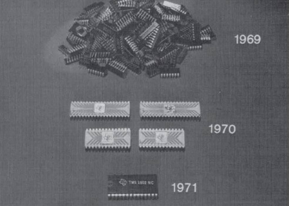
Increasing integration meant that it would soon be possible to combine the four chips in the ‘Pocketronic’ into one. But TI was beaten in the race to create the first calculator on a single chip in November 1970 by Texas rival Mostek, with the MK6010. “Electronics” magazine reported in Feb 1971:
The apparent winner in the race to produce a calculator on a chip has hit the wire. Mostek Corp., of Carrolton, Texas, is now producing such a chip for Japan’s Busicom Corp. … The 180-mil-square [4.6 mm-square] chip contains the logic for a four function 12-digit calculator – more than 2,100 transistors in 360 gates plus 160 flip-flops.
The MK 6010, like the first microprocessor, the Intel 4004, was made under a ‘… sales arrangement with the Nippon Calculating Machine Co. of Tokyo for use in Nippon’s line of Busicom calculators.’
It took a year for TI to respond. In November 1971 they announced their own ‘calculator-on-a-chip’, the TMS 1802NC (not to be confused with the RCA 1802 microprocessor, which is a later, unrelated, design). What distinguished the TMS 1802NC was that it was programmable. According to TI’s marketing10:
The device is totally programmable, the “program” read-only memory, timing sections, control section and input/output decoders can be programmed to achieve different computing characteristics . This approach offers maximum design flexibility at very low cost.
When TI said ‘totally programmable’ they meant ‘programmable at the factory’, as the program was fixed during manufacturing in a ‘mask programmable’ Read-Only-Memory. According to the patent for the 1802:
The programmable read only memory and the programmable logic arrays are easily modified by changing only the gate-insulator mask for the metal-insulator-semiconductor integrated system embodiment during the fabrication process.
In other words, calculator designers could pay TI to alter this program for their own products, but the program was fixed for end users.
The cost advantages of the microcontroller approach are soon apparent when we compare it with the Intel 4004 microprocessor, which was also launched in November 1971. The 4004 cost $60 and needed multiple support chips to create a calculator. By contrast, the 1802 sold for $20 in quantities of 10,000 or more (although it was as much as $150 for individual parts). The 4004 was considerably more sophisticated, but the price difference made the 1802 a compelling design.
TI was aggressive in setting the $20 price point for the 1802. As Ken Shirriff has noted, the die size of the 1802 was much bigger than the Intel 4004. With a bigger die, the 1802 was able to use 7,000 transistors (although see this footnote11 on transistor numbers), when compared to only 2,300 for the 4004 and 2,100 for the MK6010.
According to TI engineer Gary Boone, who led the early development of the 1802, the genesis of the project came, not from a desire to cut costs or compete with Mostek, but rather to make the most of the engineering resources that TI had available and which had been focused on developing custom integrated circuits for multiple TI calculator customers:
The individual requirements differed in detail, but in principle and in overall function, they were almost identical. So, what goes through your mind is, “I’m tired of doing this. I’m working long hours. My family is not happy. I’ve got to find a better way to do this.”
… that’s the genesis of particularly the TMS 100 microcontroller chip: it came out of boredom, high demand and a vision of commonalities that were being inefficiently served by deploying huge teams with many chips.
One can get a sense of the problems that the TI teams had from the layout of the TMX1795 microprocessor that they built at around the same time. Quoting Ken Shiriff12:
… Texas Instruments didn’t seem to put much effort into the layout, which [Intel engineer Stan] Mazor calls “pretty sloppy techniques” and “throwing some blocks together”. While the 4004 and especially the 8008 are densely packed, the TMX 1795 chip has copious unused and wasted space.
It seems likely that the TI teams simply didn’t have time to refine the design for any one customer. They needed to get it done and move on to the next.
Working with Daniel Baudouin, TI’s MOS Marketing manager, Boone compiled a matrix of customer requirements, and then set out to create a design that would meet as many of those requirements as possible. The 1802 was the result, designed by Boone and a small team of around six engineers. Boone also worked on the TI 1795X, the same design that would also provide the architecture for Intel’s first 8-bit microprocessor design, the Intel 8008. Boone’s testimony on his work on the 1802 would be central to TI’s efforts to overturn the Hyatt patent.
There has been some debate around whether the 1802 design qualifies as a ‘microcontroller’, rather than a ‘fixed function’ calculator chip.13 As we’ve seen, the program ROM in the 1802 could be changed, and TI did offer variants by changing that program. The documentation that TI created for engineers using the 1802 (which by then had then been renamed to be the TMS 0102, part of the TMS 0100 series) shows that it was primarily designed to be used in calculators. Most significantly, the input / output pins of the 1802 were designed to drive a calculator display and to support reading from a simple calculator keyboard.
However, the key patent for the 1802, U.S Patent No. 4,074,351, focuses on its use in calculators, but briefly discusses its use in a much broader range of devices:
For example, the calculator system may be programmed to perform meter functions such as for a digital voltmeter ,event counting, meter smoothing, taxi-fare meter, an odometer, scale meter to measure weight, etc.
Perhaps one way of settling the debate is to say that the 1802 was a microcontroller but not a ‘general purpose’ one. In other words, it was a programmable computer on a chip but one which had a fairly narrowly defined set of applications.
The 1802 was innovative in how it was designed. According to Boone:
We relied on our own simulations and our own software. Today it would be called register transfer model simulating. We modeled the [instruction] processing and program and data and input and output resources on this chip. That basically permitted us to test the design at a high level, before our silicon existed. That was a leap, an innovation in design methodology.
Wireless World reported on the 1802’s architecture and capabilities:
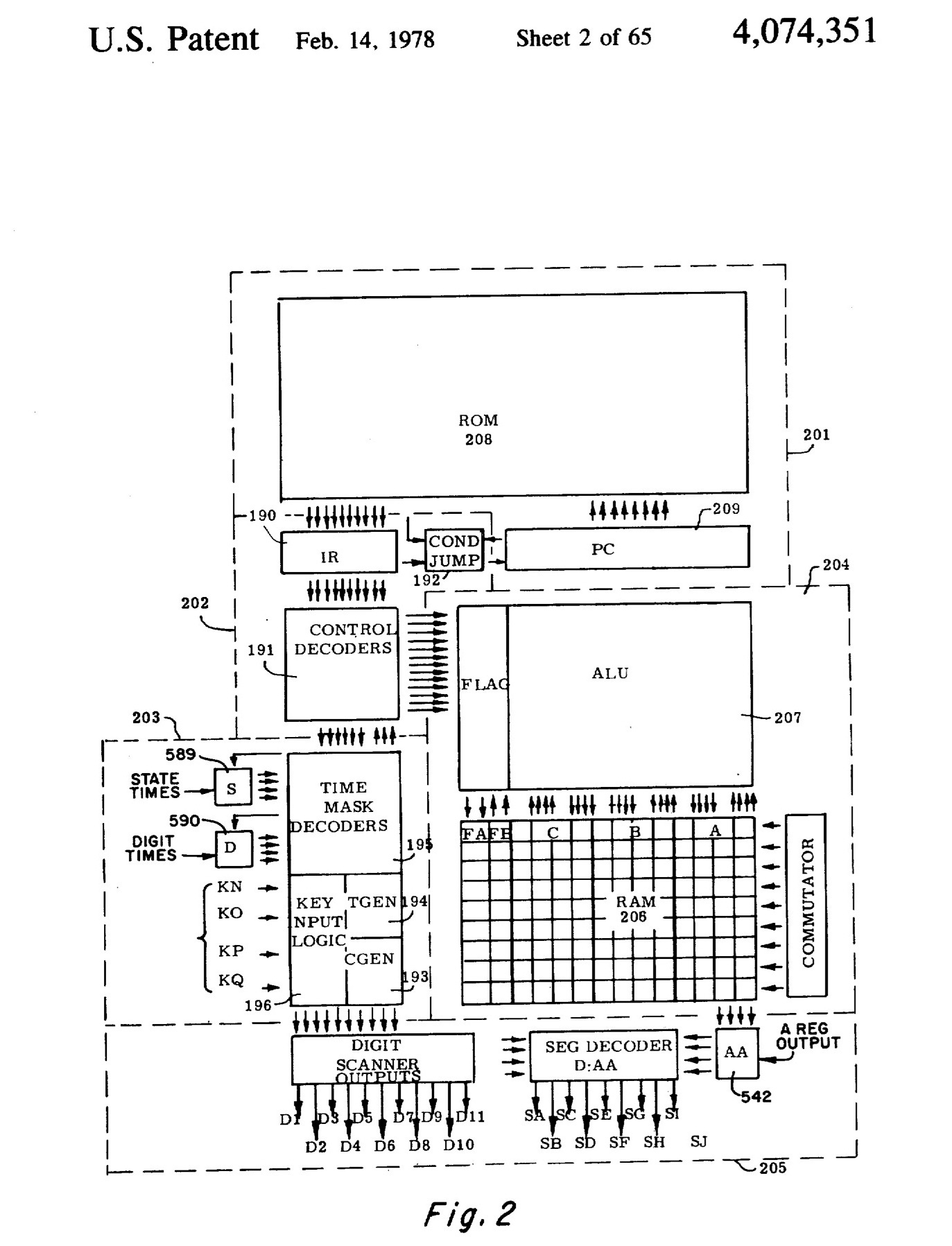
The i.c. contains an eight-digit b.c.d. arithmetic logic unit; a three-register 182-bit random access store; a 3520-bit read-only memory for holding the programme; and timing, output, and control decoders. Floating-point or fixed-point operation calculations can be performed and there is automatic round-off of numbers and leading zero suppression. Arithmetic and control operations are based on a 4μs single-phase clock system.
So that’s 182 bits of RAM (organised as 3 x 13 4-bit BCD (Binary-Coded-Decimal)14 registers plus 2 x 13 bit flags registers), and 3520 bits of ROM (arranged as 320 instructions x an 11-bit instruction length). It’s interesting to compare this with the memory used in the Intel 4004-based Busicom 141-PF calculator, which had 640 bits of RAM and 8196 bits of ROM. The Busicom offered more functionality, but even so, squeezing a calculator into the small memory footprint of the 1802 represents an impressive achievement. It was thought sufficiently noteworthy at the time for the whole program, in both binary and assembly language form, to be listed in the key patent for the 1802 (see the notes to this post for this patent).
If imitation is the greatest form of flattery then TI should have been flattered. Mostek, who had beaten TI to the first single chip calculator, followed that design up with the MK 5020, a clone of the 1802.
The 1802 was soon used in calculators from both the US and Japan. TI itself used it in its own first calculator design, the TI-2500 Datamath, in July 1972. One of the most creative uses of the 1802, though, came from the UK. Squeezing extra capabilities out of low-cost hardware was Clive Sinclair’s speciality. Attracted by the low price of the 1802, he assigned the task of developing a new calculator to Chris Curry. Curry has told the story of flying across the Atlantic on New Year’s Day 1972, still hung over from Sinclair’s New Year’s Eve party, to collect three samples of the 1802 from a TI factory in Texas.
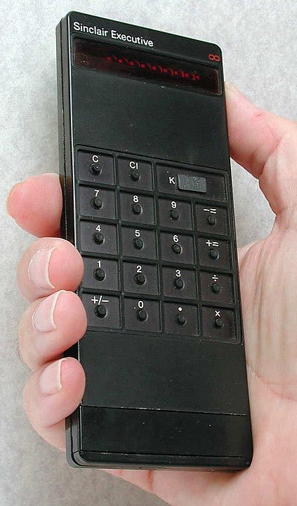
Returning to the UK, Curry built the ‘Sinclair Executive’ calculator around the 1802. The 1802 was built using a PMOS fabrication process and so was much more power hungry than later CMOS based designs. The Sinclair team dramatically reduced the power consumption of the Executive by supplying power to the 1802 in 1.7-microsecond pulses, with the capacitance of the chip retaining data during periods when there was no power. This extended battery life to around 20 hours whilst using small ‘hearing aid’ batteries, which in turn allowed the Executive to support a ‘slimline’ form factor with a thickness of just 9 millimetres.
The low price of the 1802 enabled the Sinclair Executive to be launched with a price of £79.95 (inexpensive for the time, but still equivalent to over £1,000 or $1,600 in 2024). Its innovative design and lower cost made it a huge success and allowed Sinclair to build a calculator business that, at its peak, was making over 100,000 units a month.
This wasn’t the end of Sinclair’s innovation using TI calculator chips. In 1974 he launched the Sinclair Scientific, using one of the 1802’s successors, the TMS 0805, which would show just what was possible with just 320 instructions by cramming scientific and trigonometric functions into that tiny space. Ken Shiriff has reverse-engineered the program to show how it was done, and built a simulator for the calculator, emulating what Ken calls TI’s ‘crazy’ 11-bit opcodes.15.
In a twist of history, Chris Curry would later go on to found Acorn Computers, the firm that developed the original ARM architecture. Later versions of the ARM architecture would become one of the most popular processor designs in the 32-bit microcontroller market. TI’s adoption of the ARM architecture and use of ARM-based TI System-on-Chip designs in early 3G mobile phones from Nokia and others would be a key step in Arm’s journey to market success. TI would also provide ARM with a future CEO, Warren East, when it closed its UK manufacturing plant in Bedford in 1994.
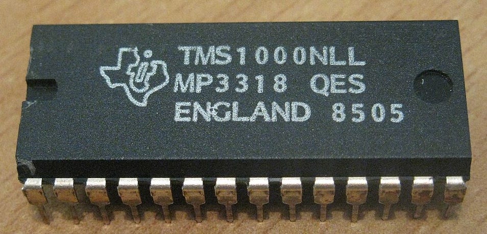
The TMS 1802 and the other members of the TMS 0100 series were successful in the calculator market, but there were opportunities for TI to expand the use of the ‘computer-on-a-chip’ into other applications where its low cost would be a compelling proposition. So the TMS 0100 series was followed by the TMS 1000 series, which was designed to be used both in calculators and in a wider range of control applications. Launched in 1974, the TMS 1000 used a 4-bit processor architecture and would sell for as little as $2 in volume.
Let’s look at the architecture of the TMS 1000 series. It’s interesting to see what simplifications were necessary to enable it to fit into such a cheap device.
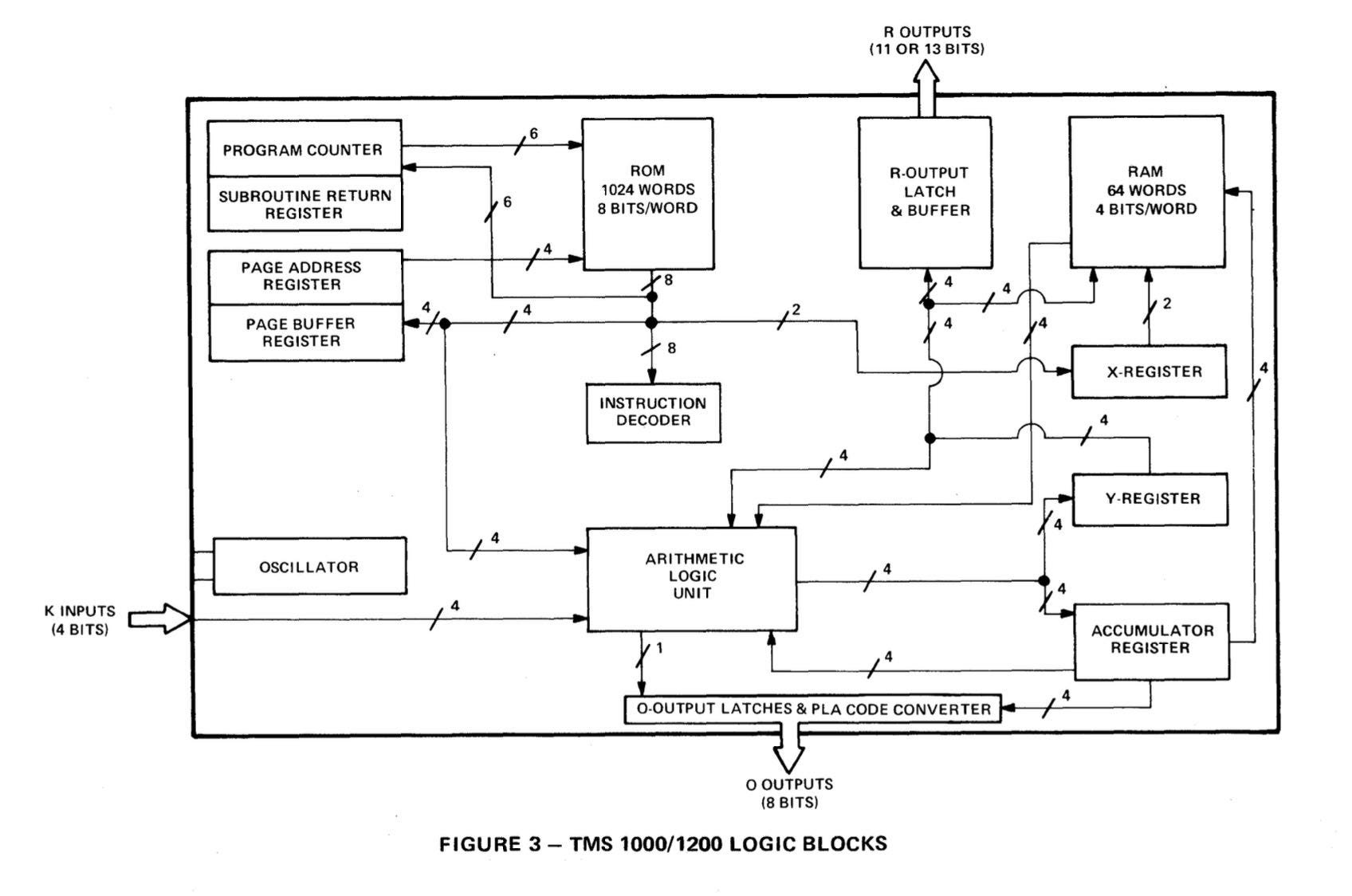
The first thing to emphasise about both the TMS 0100 and TMS 1000 series, which distinguishes them from microprocessors, is that they cannot access external RAM or ROM. The basic TMS 1000 provided 1,024 x 8 bits of ROM and 64 x 4 bits of RAM (or up to double this amount of RAM and ROM for some members of the series) and that’s it. If your design needed more memory than this then you’d needed a microprocessor based system, with the extra costs and complexity involved. With no option to access external memory, most of the pins on the TMS 1000’s package are available to read and write signals from external hardware, such as a keyboard or display.
With so little RAM it wouldn’t make sense to try to load programs into RAM so the TMS 1000 series, like the TMS 0100 series, are Harvard architecture designs : instruction and data memory are completely separate.
The instruction set of the TMS 1000 series introduces an interesting feature when compared to more familiar microprocessor designs. It’s ‘programmable’. It comes with a ‘standard’ instruction set which we will describe in a moment. However, instructions are, in part, implemented by what is known as a ‘Programmable Logic Array’, another form of ‘mask-programmable’ ROM, which can be changed for individual customers. From the TMS 1000 series Data Manual:
The programmable instruction decode is defined by the instruction PLA. Thirty programmable-input NAND gates decode the eight bits of instruction word. Each NAND gate output selects a combination of 16 microinstructions. The 16 microinstructions control the arithmetic unit, status logic, status latch, and write inputs to the RAM.
As an example, the “add eight to the accumulator, results to accumulator” instruction can be modified to perform a “add eight to the Y register, result to Y” instruction. Modifications that take away an instruction that is not used very often are desirable if the modified instructions save ROM words by increasing the efficiency of the instruction repertoire.
When we look at the architecture of the TMS 1000, we can see measures taken to reduce the number of transistors needed for the design, to keep manufacturing costs down. Just a few examples:
-
Paged RAM : The TMS 1000 has a 4-bit accumulator (A), a 4-bit memory pointer register (Y) and a 2-bit register (X) that provides the upper two bits of any RAM address. As an example of how memory access works in practice, there is an instruction ‘TAM’ that transfers A to the memory address X * 16 + Y. So the TMS 1000 implements segmented or paged memory addressing with only 64 ‘nibbles’ or RAM.
-
Paged ROM : Instruction addresses are also segmented with an address being derived from a 6-bit program counter plus, in its higher four bits, a 4-bit ‘page register’. Programs stay in a 64-byte ‘page’ unless they branch to another page.
-
Single level ‘stack’ : There was no stack, but a register was provided to store the program counter on a subroutine call, allowing for just a single level of calls.
-
Pseudo-Random Program Counter Increments : The program counter doesn’t increase by one after executing each instruction but instead changes to a value in a predetermined, but random-looking sequence.
The last example may look particularly strange:
The Program Counter is implemented as a feedback shift register rather than as a binary counter. This means that the logically consecutive program memory locations do not reside physically consecutive in the program memory.
A feedback shift register16 would have needed fewer gates than a binary counter. The mapping of logical location to physical location is given in the table below (from Adam Osborne’s 4 & 8 bit Microprocessor Handbook).

So, for example, after executing an instruction at location #37 the next instruction to execute is at location #2F.
I’m sure for many readers the TMS 1000 instruction set looks infuriating! Ease of programming lost out to keeping the cost low! Still, I really admire the creativity of the TI team in finding ways to keep the TMS 1000 small.
The TMS 1000 series soon found its way into a wide range of devices, with TI often ‘eating its own dog food’ by using the chips in its own products. TI helpfully provided a schematic of how the TMS 1000 might be used in a simple ‘terminal’ device with a keyboard and 11-digit display.

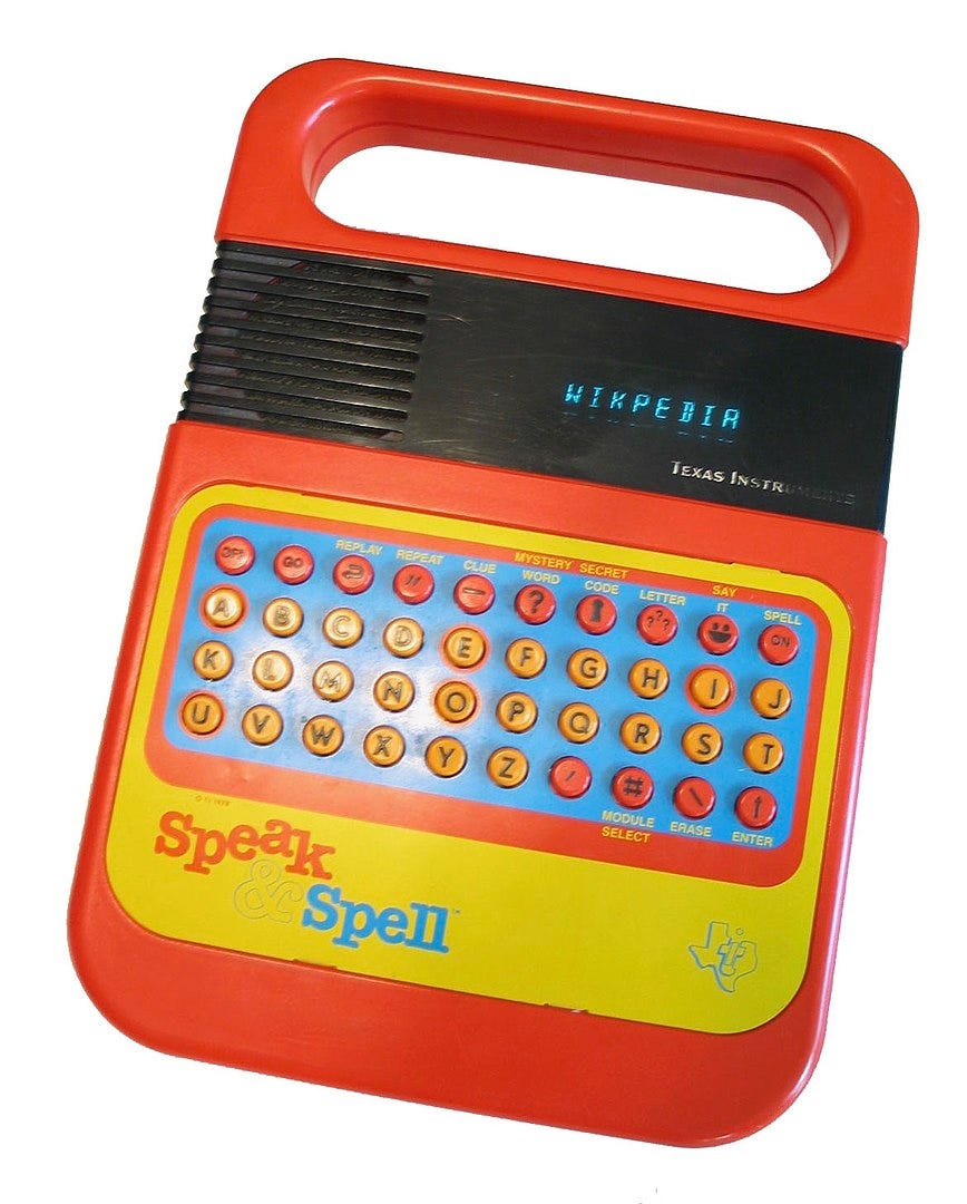
Famously, TI used it in its own ‘Speak and Spell’ educational toy. The Speak and Spell would play a synthesised set of 200 words and invite the child to spell them on a keyboard. A TMS 1000 microcontroller controlled the operation of the toy, reading the keyboard and handling the display. The hard work of voice synthesis, though, was done by another TI chip, the TMS 5100, connected to two 128 kbit ROM chips.
The popularity of TI’s microcontrollers soon attracted competition. As it became possible to implement more sophisticated designs on a single low-cost integrated circuit, the 4-bit architecture of the TMS 1000 became an unnecessary constraint. Some competitors would build 4-bit designs, whilst others would move to more powerful 8-bit architectures. We’ll look at these competitors and what happened next in Part 2 of the ‘Early History of the Microcontroller’.
Before we leave the TMS 1000 completely though, although it is no longer manufactured, there is an open-source implementation of the design available from the OpenCores website17. As is often the case, popular technology never completely disappears.
After the break, the references, links to more ‘further reading’ on early TI microcontrollers, including original documentation and key patents.


